
Big Trouble in Little Interconnects
Interconnects—those often nanometers-vast metallic wires that backlink transistors into circuits on an IC—are in want of a major overhaul. And as chip fabs march towards the outer reaches of Moore’s Law, interconnects are also turning out to be the industry’s choke point.
“For some 20-25 years now, copper has been the steel of preference for interconnects. Nonetheless we’re achieving a stage where the scaling of copper is slowing down,” IBM’s Chris Penny, instructed engineers final month at the IEEE Intercontinental Electron System Conference (IEDM). “And there is an opportunity for alternate conductors.”
Ruthenium is a foremost candidate, but it is not as straightforward as swapping one metallic for another, according to exploration described at IEDM 2022. The procedures of how they’re fashioned on a chip will have to be turned upside down. These new interconnects will will need a different form and a increased density. These new interconnects will also require far better insulation, lest sign-sapping capacitance acquire away all their gain.
Even the place the interconnects go is established to modify, and shortly. But research are setting up to demonstrate, the gains from that shift arrive with a certain charge.
Ruthenium, prime vias, and air gaps
Between the replacements for copper, ruthenium has obtained a pursuing. But exploration is demonstrating that the aged formulas used to create copper interconnects are a drawback to ruthenium. Copper interconnects are developed employing what is named a damascene system. Very first chip makers use lithography to carve the condition of the interconnect into the dielectric insulation earlier mentioned the transistors. Then they deposit a liner and a barrier substance, which helps prevent copper atoms from drifting out into the rest of the chip to muck items up. Copper then fills the trench. In point, it overfills it, so the excessive need to be polished absent.
All that further things, the liner and barrier, consider up house, as substantially as 40-50 percent of the interconnect quantity, Penny informed engineers at IEDM. So the conductive section of the interconnects are narrowing, specifically in the ultrafine vertical connections amongst levels of interconnects, raising resistance. But IBM and Samsung researchers have observed a way to make tightly-spaced, reduced-resistance ruthenium interconnects that really don’t need to have a liner or a seed. The approach is named spacer assisted litho-etch litho-etch, or SALELE, and, as the name implies, it depends on a double assisting of intense-ultraviolet lithography. As an alternative of filling in trenches, it etches the ruthenium interconnects out of a layer or metal and then fills in the gaps with dielectric.
The scientists reach the most effective resistance making use of tall, slim horizontal interconnects. Nonetheless, that raises capacitance, investing absent the profit. The good thing is, thanks to the way SALELE builds vertical connections termed vias—on prime of horizontal interconnects as a substitute of beneath them—the spaces among slender ruthenium traces can quickly be filled with air, which is the most effective insulator readily available. For these tall, slim interconnects “the possible profit of introducing an air hole is huge… as significantly as a 30 % line capacitance reduction,” explained Penny.
The SALELE course of action “provides a roadmap to 1-nanometer procedures and past,” he mentioned.
Buried rails, back again-side energy delivery, and very hot 3D chips
As early as 2024, Intel ideas to make a radical change to the spot of interconnects that have power to transistors on a chip. The scheme, identified as again-side power shipping and delivery, usually takes the network of ability delivery interconnects and moves it beneath the silicon, so they technique the transistors from down below. This has two major positive aspects: It allows electricity to stream by broader, considerably less resistive interconnects, primary to significantly less ability decline. And it frees up space higher than the transistors for sign-carrying interconnects, this means logic cells can be lesser. (Scientists from Arm and the Belgian nanotech analysis hub Imec stated it all here.)
At IEDM 2022, Imec scientists came up with some formulas to make back again-side electric power function much better, by finding ways to shift the finish factors of the ability shipping and delivery community, identified as buried electric power rails, nearer to transistors without messing up these transistors’ electronic homes. But they also uncovered a somewhat troubling difficulty, back-facet electricity could lead to a develop-up of heat when used in 3D stacked chips.
Very first the very good news: When imec scientists explored how significantly horizontal length you need to have amongst a buried energy rail and a transistor, the remedy was really significantly zero. It took some further cycles of processing to ensure that the transistors had been unaffected, but they confirmed that you can create the rail correct beside the transistor channel region—though even now tens of nanometers down below it. And that could suggest even smaller logic cells.
Now the terrible information: In different investigation, imec engineers simulated numerous versions of the exact same foreseeable future CPU. Some experienced the sort of electric power supply community in use these days, termed entrance-side power supply, in which all interconnects, both info and power, are created in layers previously mentioned the silicon. Some had again-side energy shipping and delivery networks . And one was a 3D stack of two CPUs, the base owning back-side ability and the top rated having front-aspect.
Back-facet power’s benefits were confirmed by the simulations of the 2D CPUs. When compared to front-facet shipping, it lower the decline from electrical power shipping in fifty percent, for illustration. And transient voltage drops have been significantly less pronounced. What’s more, the CPU region was 8 per cent scaled-down. Nonetheless, the best component of back again-facet chip was about 45 p.c hotter than the best section of a front-aspect chip. The likely lead to is that back-aspect ability involves thinning the chip down to the place where by it needs to be bonded to a independent piece of silicon just to stay secure. That bond functions as a barrier to the move of heat.
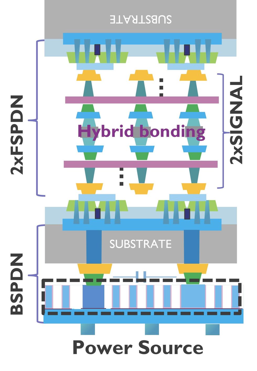 Researchers tested a circumstance exactly where a CPU [bottom grey] with a again-facet electricity supply network is bonded to a next CPU obtaining a entrance-side electrical power shipping network [top grey].
The genuine troubles arose with the 3D IC. The major CPU has to get its electrical power from the base CPU, but the lengthy journey to the best had penalties. Although the bottom CPU however had far better voltage-drop traits than a front-aspect chip, the top CPU carried out much worse in that respect. And the 3D IC’s power network ate up far more than two times the electricity that a solitary front-side chip’s community would eat. Even worse still, heat could not escape the 3D stack incredibly effectively, with the hottest section of the base die virtually 2.5 times as incredibly hot as a one front-aspect CPU. The leading CPU was cooler, but not by significantly.
The 3D IC simulation is admittedly somewhat unrealistic, imec’s Rongmei Chen advised engineers at IEDM. Stacking two or else similar CPUs atop each individual other is an unlikely scenario. (It’s substantially far more common to stack memory with a CPU.) “It’s not a really fair comparison,” he said. But it does place out some possible challenges.
From Your Site Article content
Linked Posts All-around the World wide web


