
Designing a Silicon Photonic MEMS Phase Shifter With Simulation

This sponsored report is brought to you by COMSOL.
The modern day online-related environment is generally explained as wired, but most main community details targeted visitors is in fact carried by optical fiber — not electric powered wires. Even with this, present infrastructure continue to relies on several electrical sign processing components embedded inside of fiber optic networks. Changing these components with photonic devices could raise community pace, capability, and dependability. To assist comprehend the possible of this rising know-how, a multinational team at the Swiss Federal Institute of Technologies Lausanne (EPFL) has produced a prototype of a silicon photonic section shifter, a unit that could come to be an vital developing block for the upcoming technology of optical fiber knowledge networks.
Lighting a Path Towards All-Optical Networks
Utilizing photonic products to procedure photonic indicators appears to be sensible, so why is this technique not currently the norm? “A really very good query, but actually a tricky a single to remedy!” claims Hamed Sattari, an engineer currently at the Swiss Heart for Electronics and Microtechnology (CSEM) specializing in photonic integrated circuits (PIC) with a concentrate on microelectromechanical technique (MEMS) technological know-how. Sattari was a important member of the EPFL photonics team that produced the silicon photonic section shifter. In pursuing a MEMS-primarily based solution to optical signal processing, Sattari and his colleagues are having benefit of new and rising fabrication technological know-how. “Even 10 yrs in the past, we were being not equipped to reliably make integrated movable buildings for use in these gadgets,” Sattari says. “Now, silicon photonics and MEMS are becoming additional achievable with the existing producing abilities of the microelectronics field. Our purpose is to exhibit how these abilities can be employed to completely transform optical fiber network infrastructure.”
Optical fiber networks, which make up the backbone of the net, rely on several electrical sign processing units. Nanoscale silicon photonic community factors, this kind of as stage shifters, could boost optical community pace, capability, and reliability.
The phase shifter design and style challenge is component of EPFL’s broader endeavours to establish programmable photonic parts for fiber optic data networks and room applications. These devices involve switches chip-to-fiber grating couplers variable optical attenuators (VOAs) and phase shifters, which modulate optical indicators. “Existing optical stage shifters for this application are likely to be bulky, or they go through from signal loss,” Sattari suggests. “Our priority is to build a more compact stage shifter with lower decline, and to make it scalable for use in a lot of community programs. MEMS actuation of movable waveguides could modulate an optical sign with minimal electricity use in a smaller footprint,” he explains.
How a Movable Waveguide Aids Modulate Optical Indicators
The MEMS stage shifter is a sophisticated mechanism with a deceptively straightforward-sounding goal: It adjusts the speed of gentle. To change the section of light-weight is to sluggish it down. When light is carrying a info signal, a adjust in its velocity triggers a change in the sign. Swift and exact shifts in phase will thus modulate the sign, supporting data transmission with minimal loss throughout the community. To adjust the phase of gentle traveling by way of an optical fiber conductor, or bus waveguide, the MEMS mechanism moves a piece of translucent silicon referred to as a coupler into near proximity with the bus.
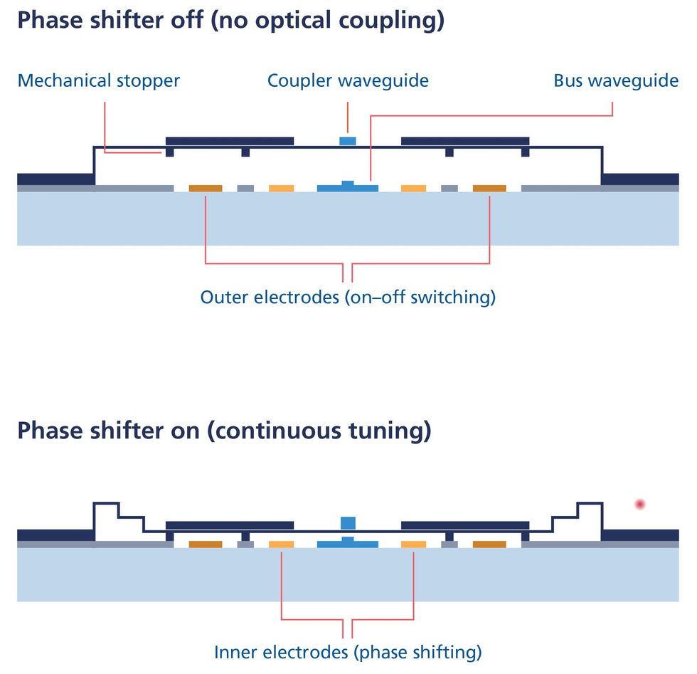
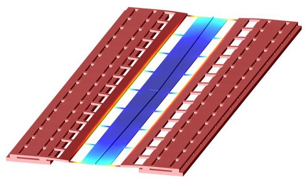
The style of the MEMS mechanism in the section shifter supplies two stages of movement (Figure 1). The first phase presents a uncomplicated on–off movement of the coupler waveguide, thereby partaking or disengaging the coupler to the bus. When the coupler is engaged, a finer vary of movement is then offered by the next stage. This permits tuning of the hole concerning the coupler and bus, which provides precise modulation of section alter in the optical signal. “Moving the coupler toward the bus is what changes the stage of the signal,” points out Sattari. “The coupler is manufactured from silicon with a higher refractive index. When the two factors are coupled, a light wave going via the bus will also pass via the coupler, and the wave will gradual down.” If the optical coupling of the coupler and bus is not carefully controlled, the light’s waveform can be distorted, likely losing the signal — and the details.
Coming up with at Nanoscale with Optical and Electromechanical Simulation
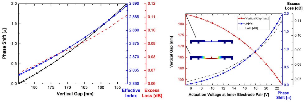
The challenge for Sattari and his staff was to layout a nanoscale system to control the coupling approach as specifically and reliably as probable. As their section shifter would use electric existing to bodily shift an optical aspect, Sattari and the EPFL crew took a two-keep track of solution to the device’s layout. Their target was to ascertain how considerably voltage experienced to be applied to the MEMS mechanism to induce a wished-for change in the photonic sign. Simulation was an critical instrument for deciding the various values that would establish the voltage vs . stage romance. “Voltage vs. phase is a sophisticated multiphysics question. The COMSOL Multiphysics software gave us lots of alternatives for breaking this significant issue into smaller tasks,” Sattari states. “We executed our simulation in two parallel arcs, applying the RF Module for optical modeling and the Structural Mechanics Module for electromechanical simulation.”
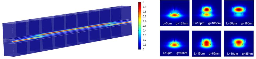
The optical modeling (Figure 2) bundled a mode examination, which decided the efficient refractive index of the coupled waveguide features, followed by a study of the signal propagation. “Our goal is for light-weight to enter and exit our gadget with only the desired adjust in its section,” Sattari states. “To aid attain this, we can establish the eigenmode of our procedure in COMSOL.”

Along with deciding the bodily sorts of the waveguide and actuation system, simulation also enabled Sattari to study worry results, such as unwelcome deformation or displacement triggered by repeated procedure. “Every choice about the layout is based mostly on what the simulation confirmed us,” he claims.
Incorporating to the Basis of Upcoming Photonic Networks
The goal of this job was to display how MEMS section shifters could be created with current fabrication capabilities. The final result is a robust and dependable design and style that is achievable with existing floor micromachined production procedures, and occupies a complete footprint of just 60 μm × 44 μm. Now that they have an recognized evidence of idea, Sattari and his colleagues glance forward to viewing their types built-in into the world’s optical info networks. “We are generating constructing blocks for the potential, and it will be gratifying to see their possible turn out to be a fact,” says Sattari.
References
- H. Sattari et al., “Silicon Photonic MEMS Period-Shifter,” Optics Specific, vol. 27, no. 13, pp. 18959–18969, 2019.
- T.J. Seok et al., “Massive-scale broadband digital silicon photonic switches with vertical adiabatic couplers,” Optica, vol. 3, no. 1, pp. 64–70, 2016.


